What Every Programmer Should Know About Memory
Today’s Hardware
Northbridge: connecting CPUs, and CPU to RAM Southbridge: connects to northbridge, PCIe, SATA, and USB
How they communicate
Communication between CPUs & RAM goes over the same bus RAM typically only has one port Communication with I/O goes through northbridge
Bottlenecks
- All communication pass through the CPU → Direct Memory Access (DMA)
- DMA requests contends with RAM access
- Single-port RAM access through Northbridge → more buses to RAM (e.g. DDR3)
- bandwidth is in high contention
How to increase memory bandwidth
- Northbridge could be connected to external memory controllers
- more bandwidth; support more memory
- integrate memory controllers into CPUs and attach memory to each CPU
- less burden on Northbridge
- memory becomes Non-Uniform Memory Architecture (NUMA)
- access memory attached to other CPUs through interconnects
- NUMA Factor: extra time needed to access remote memory
RAM Types
Static RAM (SRAM)
One cell require 6 transistors - 2 for each inverter, 2 inverters - 2 additional for overwriting values inside - Word Line: controls the access transistors; high/1 → read on bitline - Bit Line: read data from/ write data to bitline Require constant power, but the cell state is stable, no need to refresh
Dynamic RAM (DRAM)
One cell require 1 transistor & 1 capacitor State is kept in capacitor, when Access Line is raised, charge goes to Bit Line.
Leakage: takes a short time for the capacity to dissipate - DRAM must be refreshed periodically - info not directly usable, must read through a sense amplifier - reading depletes the charge → loop the output of sense amplifier back into the capacitor → costs extra energy & time - charging & draining capacitor takes time
Though with many flaws, DRAM is much cheaper to make and require less power.
Accessing DRAM
If we were to use a wire for each bit in a 4GB memory → address lines Instead, we encode the address in binary → 32 address lines = locations Require large chip area and big multiplexer
Arrange the DRAM cells in grid layout: 4GB → 65536 rows and columns Use row/column address selection → 16 row select lines and 16 column select lines Still not scalable → memory controller needs to have (16+16) * 8 = 256 for 8 RAM modules
Multiplexing the address itself
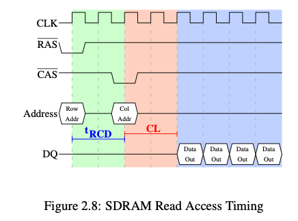
Are we transmitting the RAS and CAS over the same set of wires? Does this cut the wires by half?
A: Yes, we lower the signal and transmit RAS first, and after (-to- delay) time, we lower the line and transmit CAS. Both RAS and CAS are active-low because it’s more resistant to false-triggering due to noise. Finally, we wait for Latency (CL) before data becomes available.
Terms
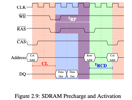
: the delay between the transmission of RAS and CAS signal CL: CAS-latency - the delay to get the data after CAS is issued Command Rate: how often the memory controller can issue commands (usually 1/2 commands per cycle) : Row precharge time (purple), the time after lowering RAS & WE and before RAS signal is sent; can overlap with memory transfer time (blue), but 1 cycle more : the time after a RAS signal and before a precharge command
Precharge
lowering RAS and WE (write-enable) line simultaneously
Require additional wire to indicate RAS vs CAS, but overall reduced the number of wires
Sequence of events
- Raise signal, transfer row address on address lines
- Wait for time, raise signal, and transfer row address on address lines
- Wait for CL (CAS-Latency) time, start receiving data
- Wait for the maximum between data transfer time (depending on DDR version, hardware), and (precharge time)
- We could then keep row open and send new CAS signal to get consecutive memory addresses; otherwise, we check if we waited long enough in Step 1-4 for to pass, wait for it to pass if not, and back to Step 1
Using Figure 2.9, suppose we have a DDR module with 2-3-2-8-T1 spec (i.e , , , , command rate=1), we have Step 1 - 4 = 8 cycles, which means RAS line has also completed precharge.
Recharge
Memory cells have to be refreshed every 64 ms, which could stall memory access.
Memory Types
- SDR: Single Data Rate
- DRAM cell array throughput = memory bus throughput
- DDR1: Double Data Rate
- transports data on the rising and falling edge
- introduced I/O buffer → 2-line data bus
- DDR2
- I/O buffer doubles the frequency → 4-line data bus
- DDR3
- 8-line data bus
Takeaways
- SRAM expensive but fast; DRAM cheap but slow
- Memory cells need to be individually selected
- number of address lines → cost of memory controller & DRAM chip
- DRAM takes time to read/write